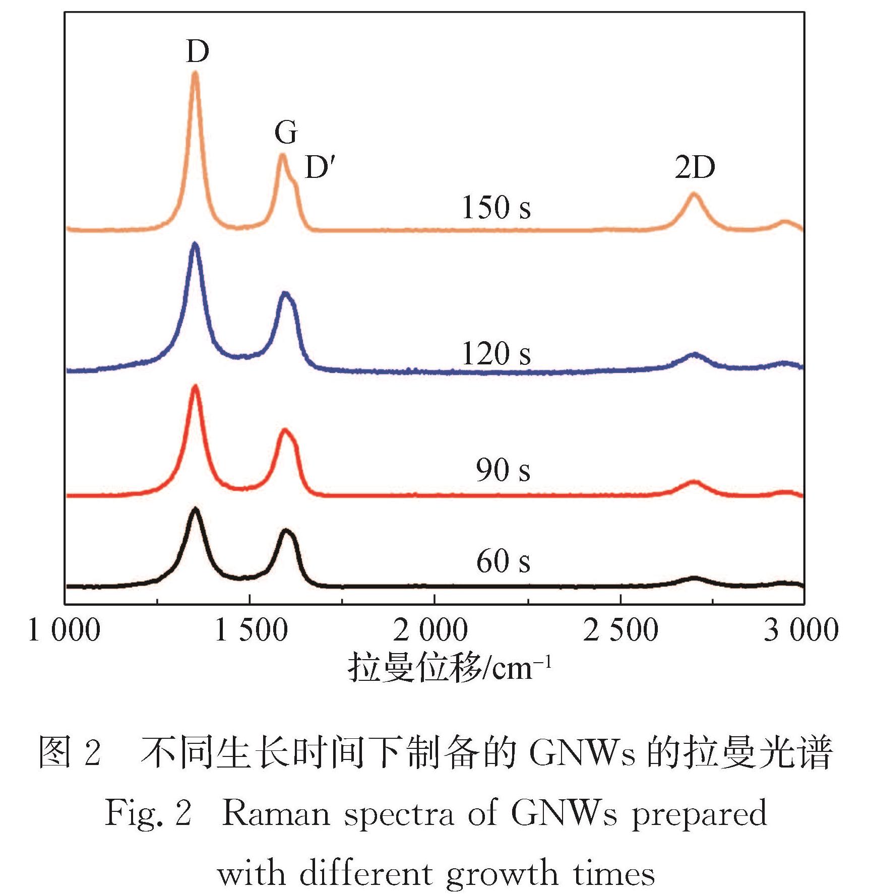
2.1 生长时间对GNWs晶体质量的影响
为了表征不同时间下制备的GNWs的晶体质量,对所制备的GNWs样品进行拉曼光谱表征,结果如图2所示.在所制备的4组GNWs样品的拉曼光谱中均出现了GR的特征峰,分别是D峰(1 350 cm-1)、G峰(1 590 cm-1)和2D峰(2 700 cm-1)[24-25].D峰主要源于GNWs的边缘态、晶体缺陷和非晶碳中的sp3杂化碳,其强度一般与GR中的缺陷数量呈正相关[25]; G峰是由sp2碳原子的面内声子振动引起的,它反映的是所制备的GNWs的晶体质量和石墨化程度[24]; 2D峰源于GR纳米片中双声子共振过程,是GR区别于石墨和类金刚石等其他碳材料的拉曼特征[25-27].G峰和2D峰的出现证明所制备的样品确实为GNWs.此外,在约1 620 cm-1的位置出现了D'肩峰,该峰源于GR纳米片中的边界声子振动,与GNWs有限的sp2碳晶粒尺寸有关.较高的D峰和D'峰的出现说明所制备的GNWs中存在较多的缺陷和边缘态,这是由GR纳米片的尺寸较小引起的[22].
图2 不同生长时间下制备的GNWs的拉曼光谱
Fig.2 Raman spectra of GNWs prepared with different growth times
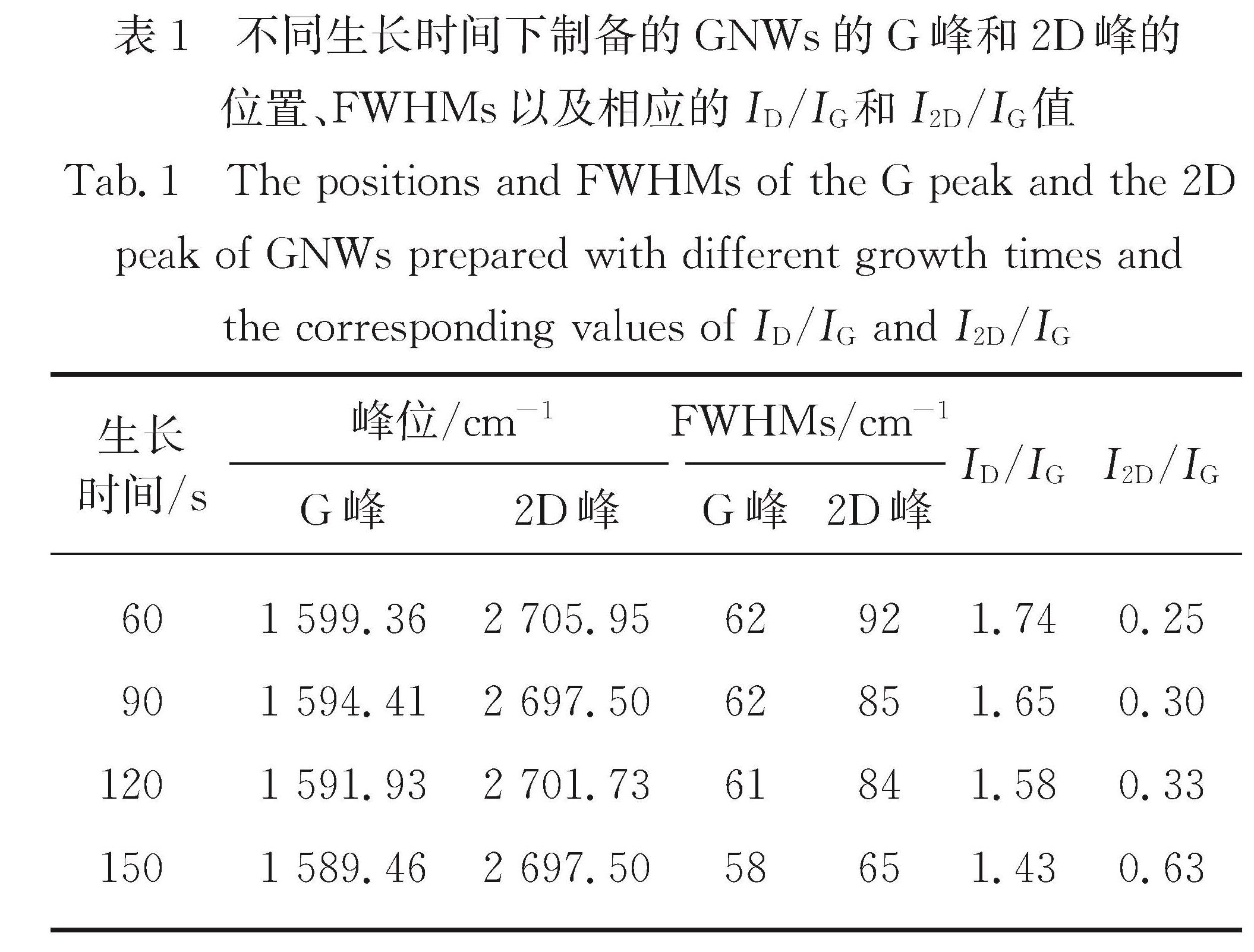
为定量分析不同生长时间对GNWs质量的影响,对图2中的拉曼光谱进行高斯拟合,计算拉曼光谱中G峰和2D峰的峰位、半高宽(FWHMs)、D峰和G峰的强度比(ID/IG)以及2D峰与G峰的强度比(I2D/IG),结果如表1所示.当生长时间从60 s延长到150 s时,G峰从1 599.36 cm-1逐渐红移到1 589.46 cm-1,说明随着生长时间的延长,所制备的GNWs的p型掺杂程度降低,这将导致GNWs的功函数随之降低[28-29].同时,G峰和2D峰的FWHMs也随着生长时间的延长而变窄,说明随着生长时间延长,所制备的GNWs的结晶度增大[25,30].ID/IG值反映了GNWs中碳原子的排布无序度以及GR纳米片的晶体尺寸大小[25].当生长时间从60 s延长到150 s时,ID/IG值从1.74减小到1.43,表明随着生长时间的延长,所制备的GNWs中sp2碳的含量增高、缺陷密度降低并且晶体尺寸增大.I2D/IG值常用于表征所制备的GR的层数,随着GNWs生长时间从60 s延长到150 s,I2D/IG值从0.25上升到0.63,说明GNWs中GR纳米片缺陷结构比例降低,且均为多层GR,这与Jiao等[22]的结论一致.
表1 不同生长时间下制备的GNWs的G峰和2D峰的位置、FWHMs以及相应的ID/IG和I2D/IG值
Tab.1 The positions and FWHMs of the G peak and the 2D peak of GNWs prepared with different growth times and the corresponding values of ID/IG and I2D/IG
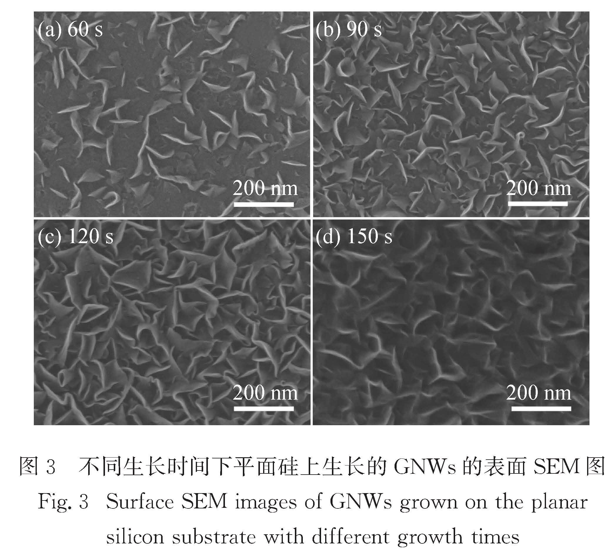
2.2 生长时间对GNWs形貌的影响
图3为不同生长时间下制备的GNWs的表面SEM图,可以看出:组成GNWs的GR纳米片基本上垂直于硅基底生长,
图3 不同生长时间下平面硅上生长的GNWs的表面SEM图
Fig.3 Surface SEM images of GNWs grown on the planar silicon substrate with different growth times
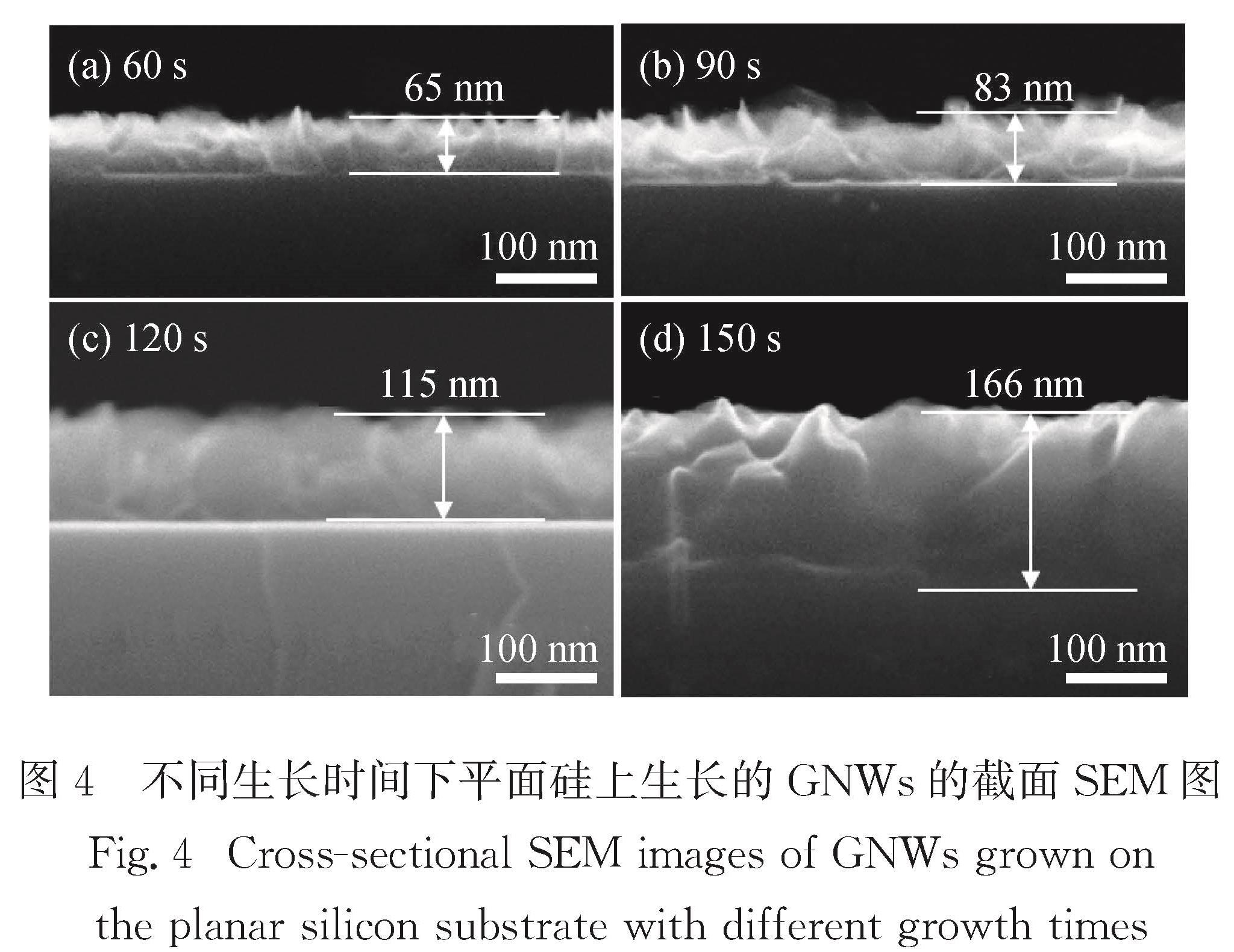
并随着生长时间的延长而相互连接形成三维网状结构.当生长时间为60 s时,GR纳米片较为稀疏,并未完全覆盖硅基底表面; 随着生长时间延长,GNWs中GR纳米片的密度增加,并完整地覆盖硅基底,同时GR纳米片的尺寸和均匀性也逐渐增加,这和拉曼光谱的分析结果一致.图4为不同生长时间下制备的GNWs的截面SEM图,可见当生长时间从60 s逐渐延长到150 s时,GNWs的厚度从65 nm 逐渐增加到166 nm.
图4 不同生长时间下平面硅上生长的GNWs的截面SEM图
Fig.4 Cross-sectional SEM images of GNWs grown on the planar silicon substrate with different growth times
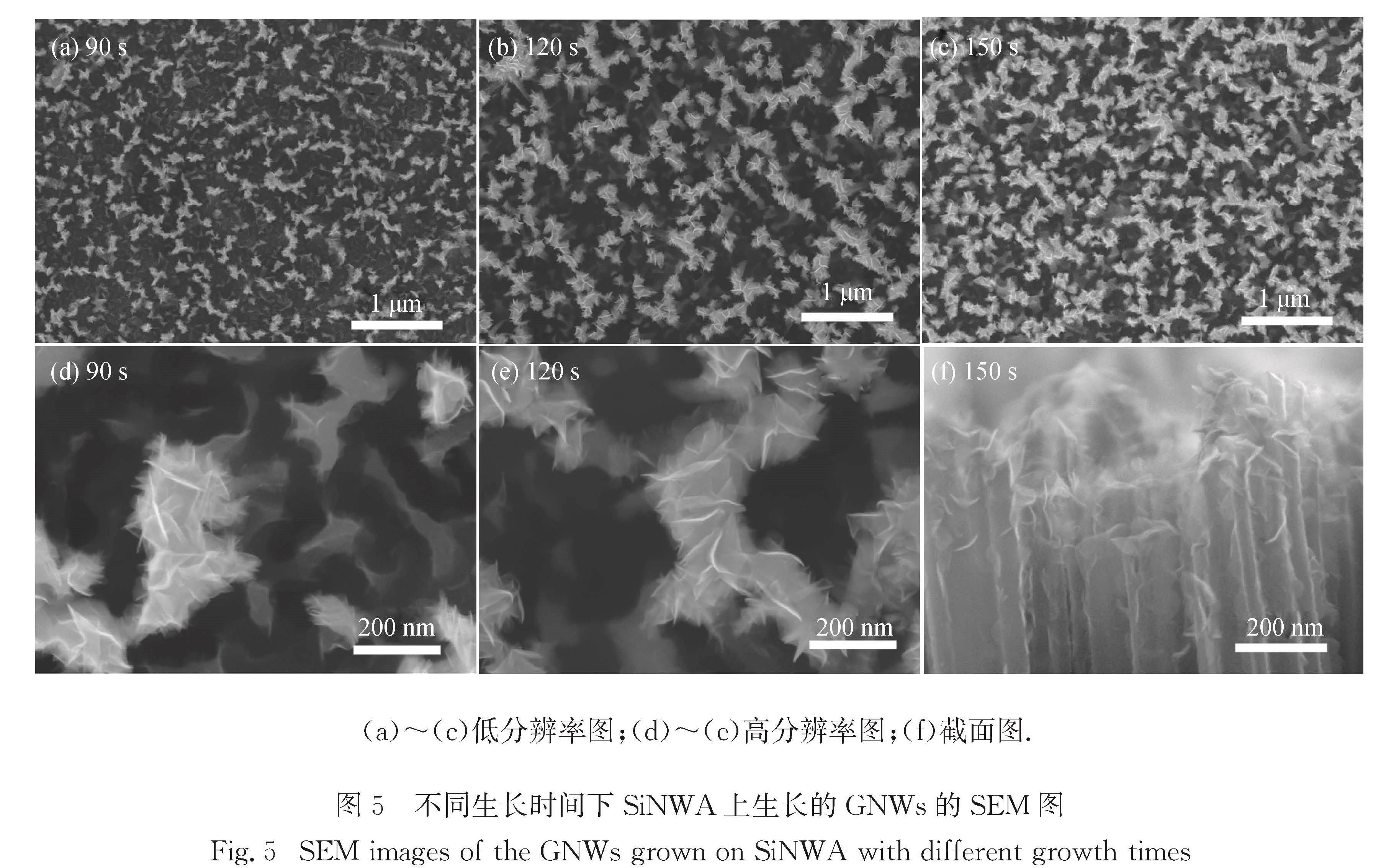
图5 不同生长时间下SiNWA上生长的GNWs的SEM图
Fig.5 SEM images of the GNWs grown on SiNWA with different growth times
相比于GNWs在平面硅上生长,GNWs在SiNWA上生长时还需要考虑其在SiNWA上的包覆情况.由低分辨率的SEM图(图5(a)~(c))可以看出,GNWs在SiNWA顶端形成了团簇(图5(a)~(c)中白色部分)并均匀分布于SiNWA表面.从高分辨率的SEM图(图5(d)~(e))可以看出,由GR纳米片组成的GNWs团簇横跨多根硅纳米线,相当于在硅纳米线之间起着桥接的作用,这有利于硅纳米线之间的载流子传输.同时,由于SEM表征以二次电子为信号,所以GNWs团簇的白色表面也验证了其良好的导电性.此外,随着生长时间从90 s延长到150 s,GNWs团簇的分布密度也逐渐增大,这显然有利于增强GNWs的导电性.从截面SEM图(图5(f))可知,GR纳米片基本上仍然保持垂直于硅纳米线侧壁生长,并与硅纳米线形成核壳结构.
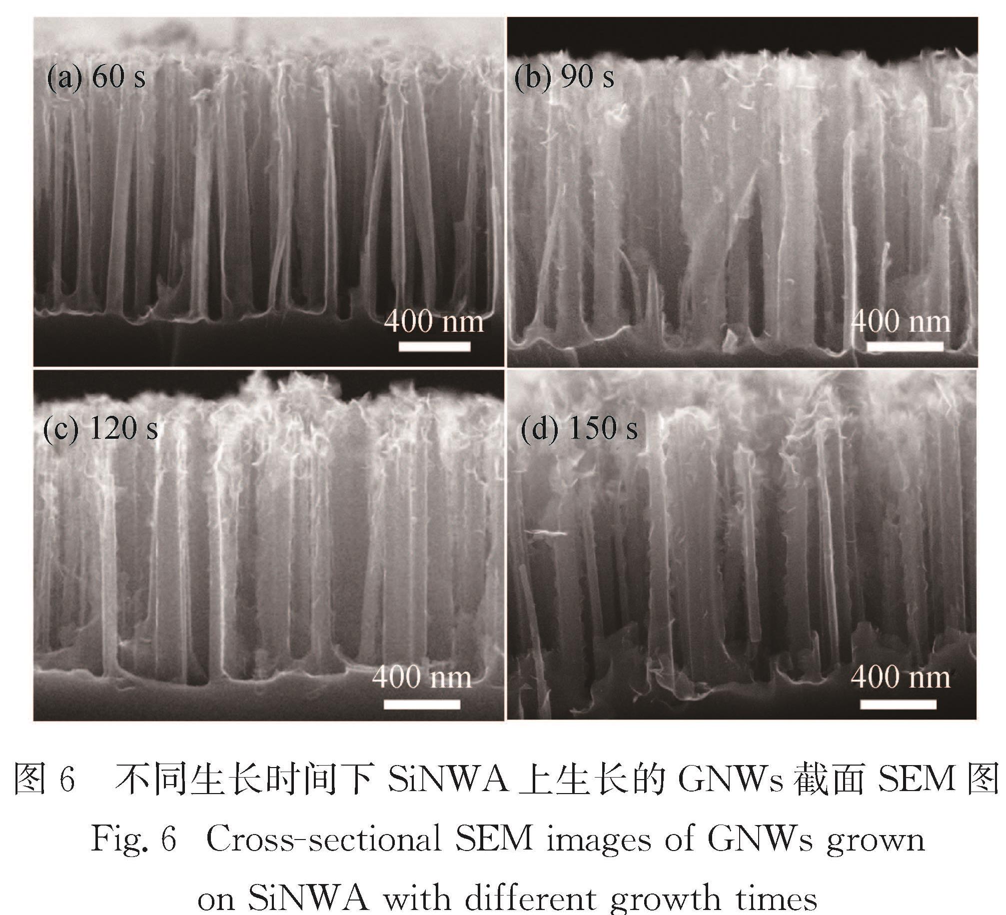
图6为不同生长时间下GNWs在SiNWA上生长的截面SEM图,可以看出:在有限的生长时间(≤150 s)内GNWs并不能完全包
图6 不同生长时间下SiNWA上生长的GNWs截面SEM图
Fig.6 Cross-sectional SEM images of GNWs grown on SiNWA with different growth times
覆SiNWA,而是自上而下沿着硅纳米线的侧壁逐渐生长,最终形成包覆SiNWA的核壳结构; 同时,GNWs向下生长并不存在一个明显的界限,而是由密到疏逐渐变化. 由于在GNWs/Si太阳能电池中,GNWs不仅作为透明导电层,还与硅形成肖特基异质结[21],所以在GNWs未完全包覆硅纳米线的情况下,生长时间越长裸露的硅表面积越小,则载流子表面复合概率越小,器件的有效结区面积越大.
简言之,GNWs在SiNWA上的生长方向是自上而下,随着生长时间的延长,GNWs的厚度逐渐增加,晶粒尺寸逐渐变大,同时在SiNWA顶端的GNWs团簇密度增大.
2.3 生长时间对GNWs的光学和电学性能的影响
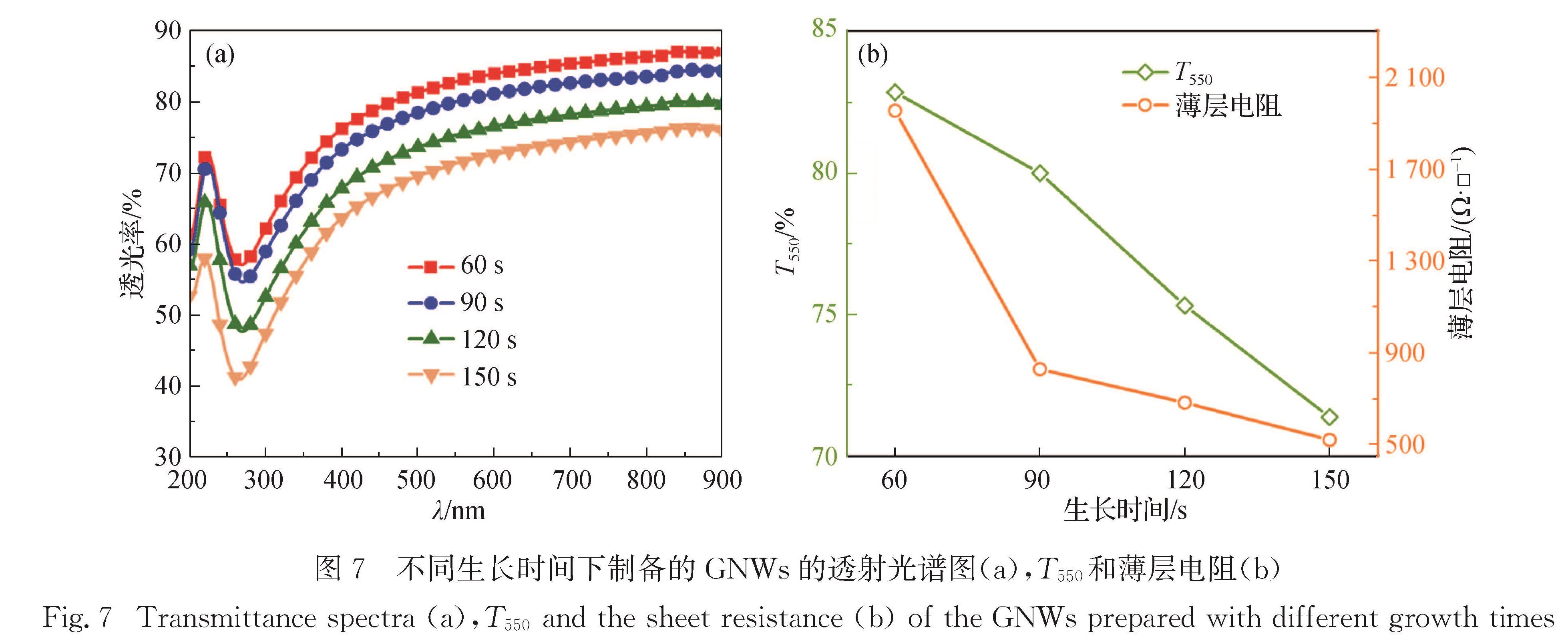
图7(a)为不同生长时间下GNWs的透射光谱图,可以看出,随着生长时间的延长,GNWs的透
图7 不同生长时间下制备的GNWs的透射光谱图(a),T550和薄层电阻(b)
Fig.7 Transmittance spectra(a),T550 and the sheet resistance(b)of the GNWs prepared with different growth times
光率逐渐降低,GNWs在波长为550 nm时的透光率(T550)由生长时间为60 s时的82.84%逐渐下降到生长时间为150 s时的71.37%.这归因于GNWs的厚度随着其生长时间的延长而增大.此外,采用霍尔效应测试表征不同生长时间下的GNWs的薄层电阻,结果如图7(b)所示:随着生长时间由60 s延长到150 s,GNWs的薄层电阻从1 953.61 Ω/□下降到519.33 Ω/□.
2.4 生长时间对电池光伏性能的影响
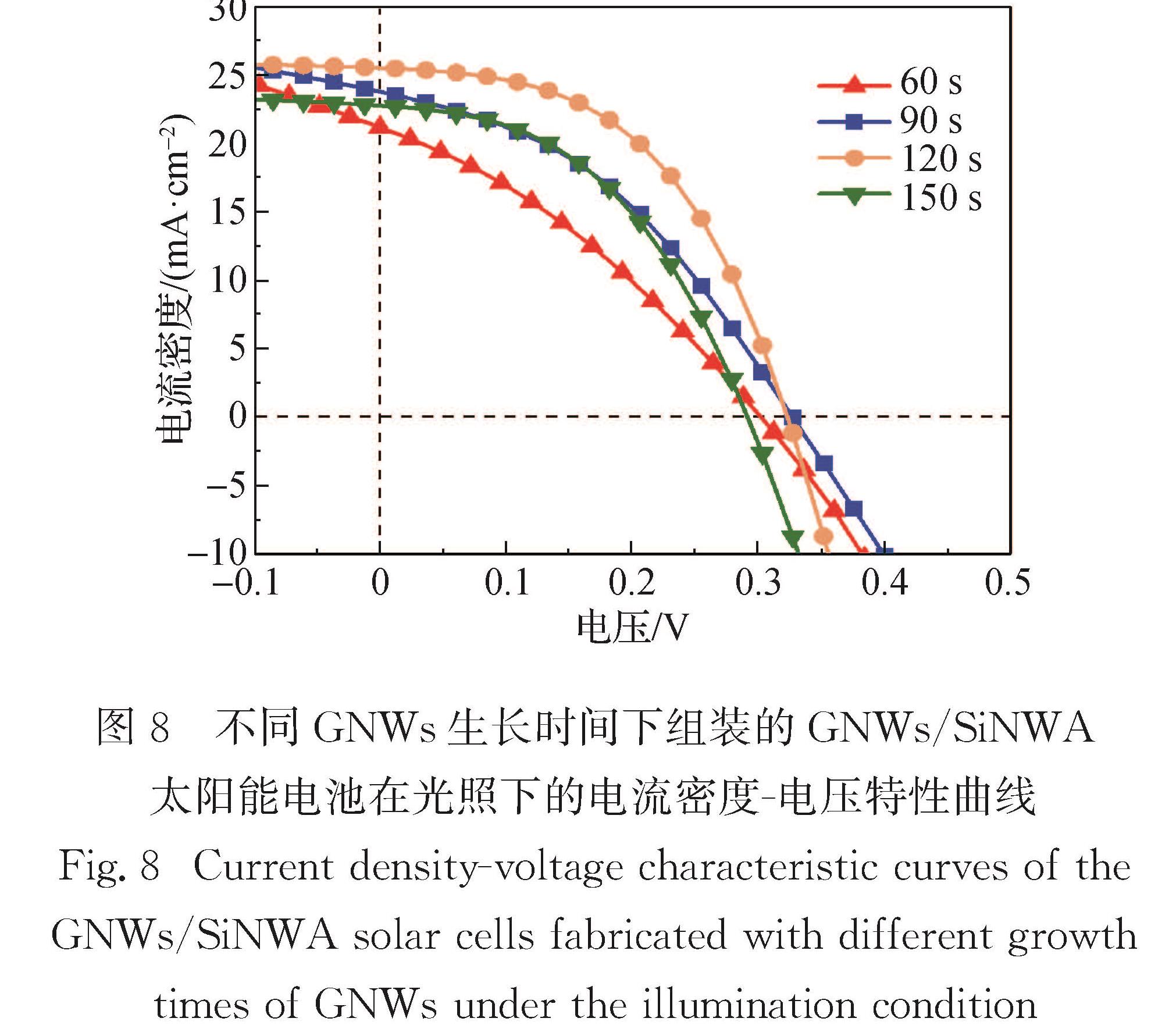
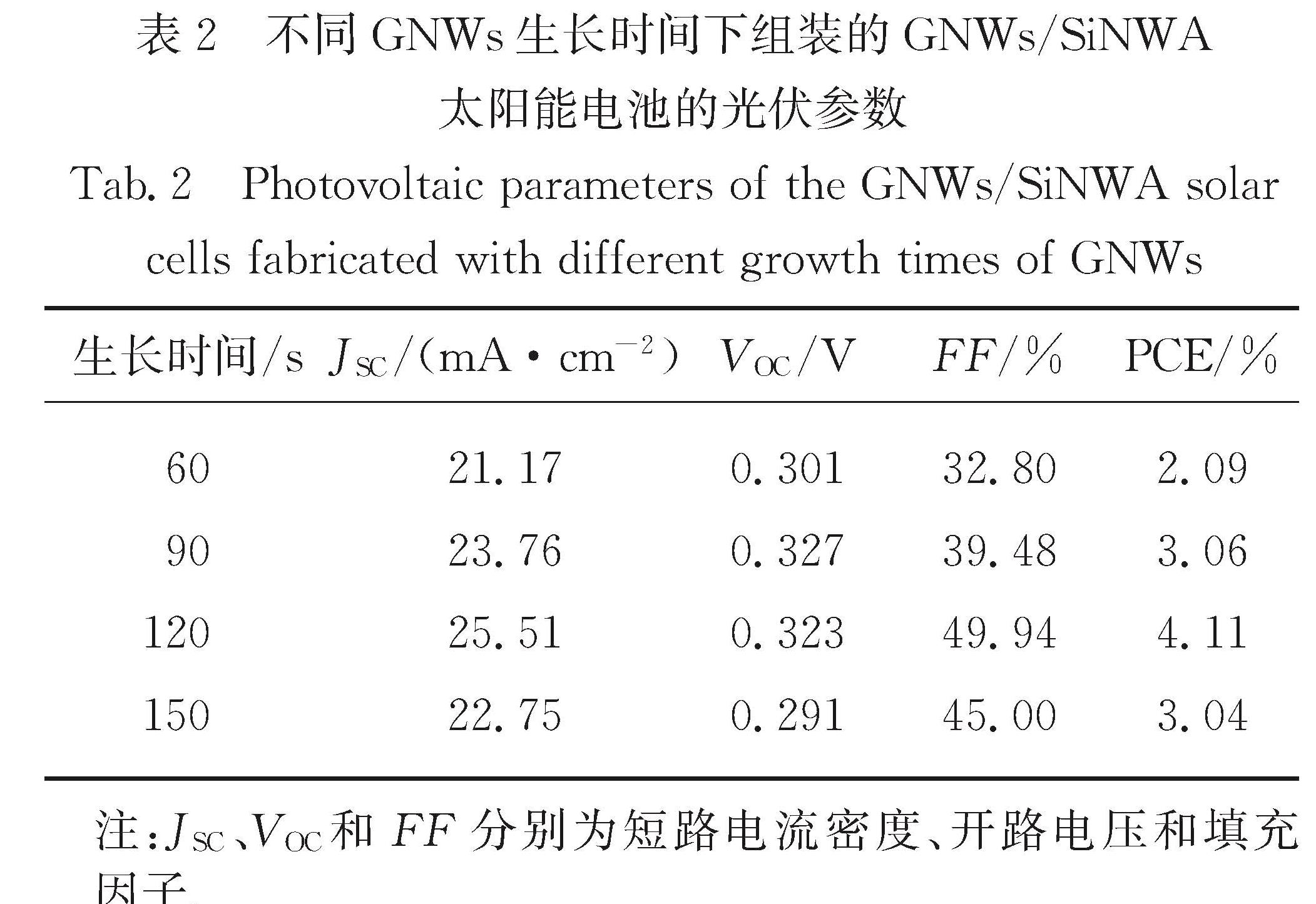
图8比较了GNWs生长时间分别为60,90,120和150 s时GNWs/SiNWA太阳能电池在光照下的电流密度-电压特性曲线,相关的光伏性能参数见表2.可以看出,随着生长时间的延长,JSC先增加后减小,并在生长时间为120 s时达到峰值25.51 mA/cm2.这归因于随着生长时间的延长,器件的有效结区面积增加,但GNWs的透光性下降,两者平衡使其在生长时间为120 s时达到JSC峰值.
图8 不同GNWs生长时间下组装的GNWs/SiNWA太阳能电池在光照下的电流密度-电压特性曲线
Fig.8 Current density-voltage characteristic curves of the GNWs/SiNWA solar cells fabricated with different growth times of GNWs under the illumination condition
表2 不同GNWs生长时间下组装的GNWs/SiNWA太阳能电池的光伏参数
Tab.2 Photovoltaic parameters of the GNWs/SiNWA solar cells fabricated with different growth times of GNWs
值得注意的是,器件的VOC仅约0.3 V,和文献[21-22]报道的GNWs/Si太阳能电池的VOC相近.与之对应的,基于转移CVD法制备的GR/Si太阳能电池的VOC一般为0.42~0.48 V[6].Deng等[31]采用PECVD法在SiNWA上生长GNWs时首先沉积一层非晶碳层来缓冲硅基底和GNWs之间的晶格失配,因此较低的VOC可能是由非晶碳层中较高的缺陷密度造成的.当生长时间从60 s延长到90 s, VOC随之从0.301 V 上升到0.327 V,可能的原因是GNWs生长初期硅基底表面会先生长一层非晶碳,其功函数比GR的低,所以在生长时间为60 s时得到了一个相对较低的VOC[25,31-32]; 而当生长时间从90 s延长到150 s时,VOC随之降低.由拉曼光谱分析可知,随着生长时间延长,GNWs的p型掺杂程度降低,使得GNWs的功函数和器件的肖特基势垒降低,最终导致VOC的降低.
此外,当生长时间从60 s延长至120 s,器件的FF从32.80%上升至49.94%,这归因于3个方面:1)生长时间较短时,SiNWA表面的非晶碳层占比较高; 2)所制备的GNWs的结晶性随生长时间延长而变好(由拉曼光谱分析可知); 3)GNWs对硅纳米线的包覆面积的增加抑制了硅纳米线表面的载流子复合.然而当生长时间进一步延长至150 s时,器件的FF略微降低到45.00%,一个可能的原因是此时GNWs的功函数降低导致肖特基势垒降低,使得太阳能电池的界面复合增强.
最终,在JSC、VOC和FF的综合影响下,当生长时间为120 s时GNWs/SiNWA太阳能电池的PCE最高,为4.11%.值得一提的是,该值是在没有化学掺杂、贵金属掺杂和界面层处理时器件的原始PCE.
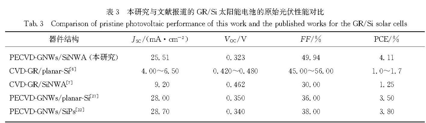
表3比较了本研究和文献报道的GR/Si太阳能电池的原始光伏性能参数,可见GNWs/SiNWA太阳能电池的原始PCE优于CVD法制备的GR分别与平面硅和SiNWA组装的太阳能电池,也优于PECVD法制备的GNWs分别与平面硅和SiPs组装的太阳能电池,这归因于GNWs/SiNWA太阳能电池拥有更高的FF.因此推测,结合GR的功函数工程以及界面工程,GNWs/SiNWA太阳能电池可以获得更高的PCE.
表3 本研究与文献报道的GR/Si太阳能电池的原始光伏性能对比
Tab.3 Comparison of pristine photovoltaic performance of this work and the published works for the GR/Si solar cells