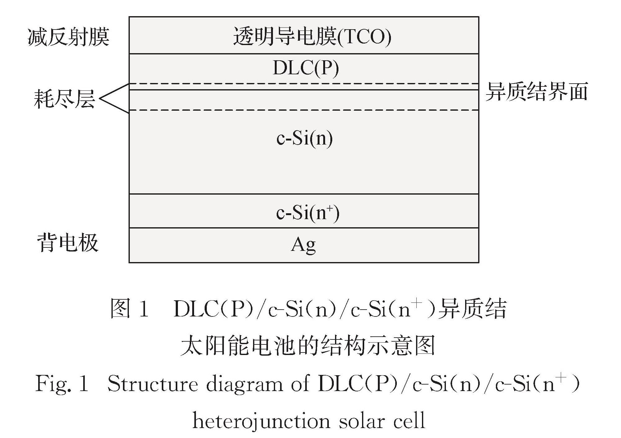
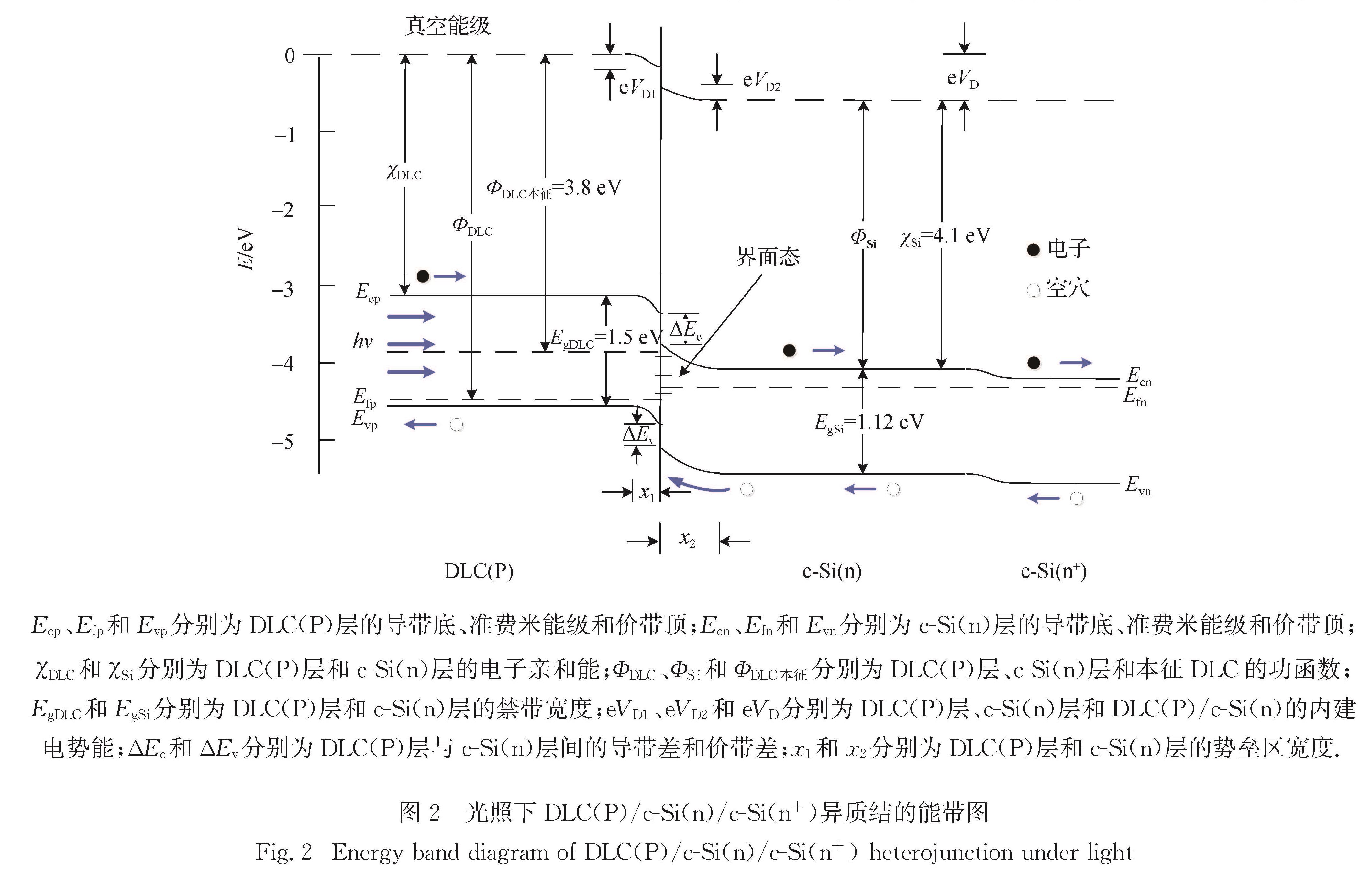
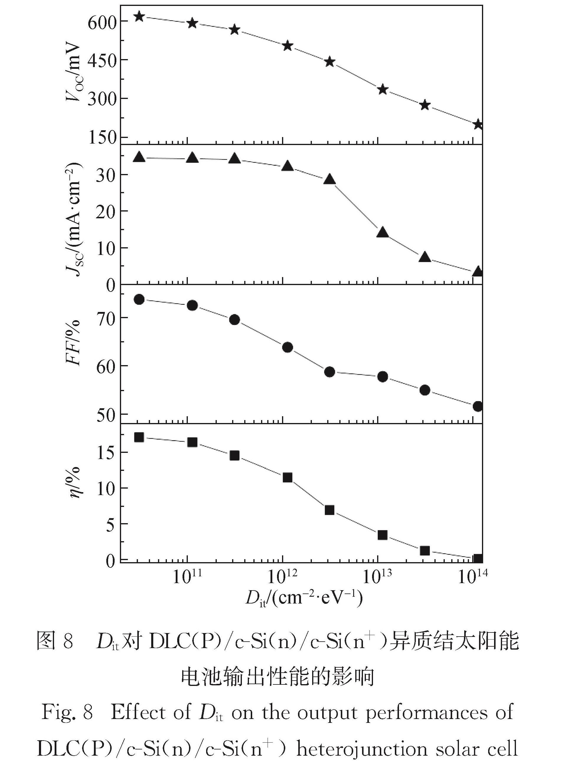
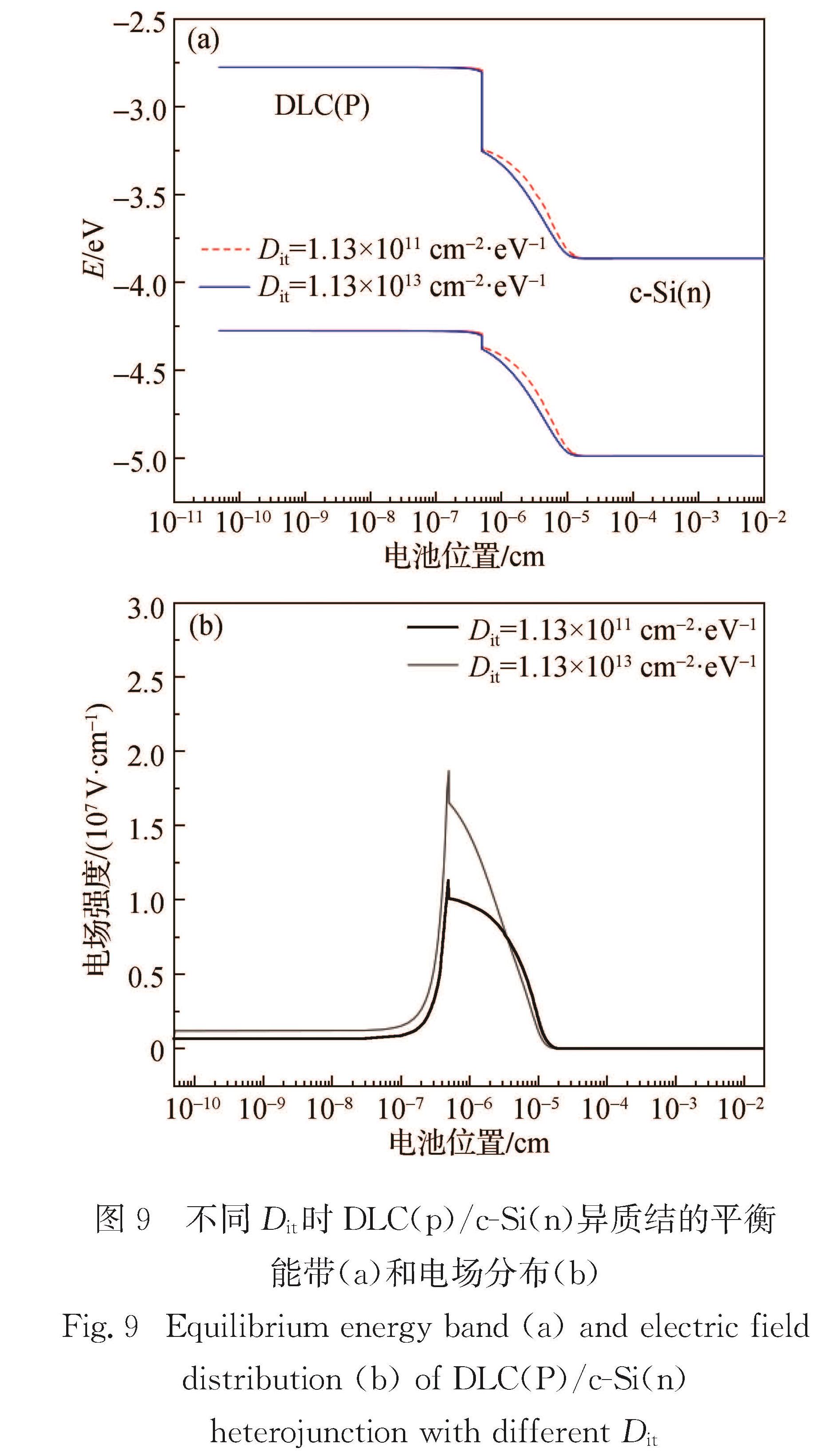
类金刚石(DLC)薄膜因其硬度高、禁带宽度可调和抗辐射性好等优点成为空间太阳能电池研究的热点材料之一.采用AFORS-HET v2.5,在AM1.5、功率密度100 mW/cm2的太阳光辐照条件下模拟DLC(P)/c-Si(n)/c-Si(n+)异质结太阳能电池的性能.通过改变P型DLC层和n型单晶硅层参数,得到太阳能电池输出性能的变化规律,并解释了性能变化的内在原因,为DLC异质结太阳能电池的性能优化提供了参考与指导.模拟结果表明:该结构太阳能电池的转换效率超过20.07%(开路电压为695.5 mV,短路电流密度为35.11 mA/cm2, 填充因子为80.56%).同时研究了DLC(P)/c-Si(n)界面缺陷密度对DLC(P)/c-Si(n)/c-Si(n+)异质结太阳能电池的影响,发现降低界面缺陷密度可以有效提高太阳能电池的性能.
Objective s:Since crystalline silicon solar cells cannot be used in high radiation environments such as the space, more and more researchers are devoted to studying new materials for solar cells. Diamond-like carbon (DLC) film, with high radiation resistance and adjustable band gap, has attracted extensive attention of researchers in the field. Although the photoelectric conversion efficiency of DLC/Si heterojunction solar cellshas been developed to be 7.9%, no greater breakthrough has been made in the conversion efficiency of the DLC/Si heterojunction solar cell.Therefore, it is necessary to systematically analyze influencing factors and mechanisms of photoelectric conversion efficiency of DLC/Si heterojunction solar cells.
Methods :In this study, the performance of TCO/DLC(P)/c-Si(n)/c-Si(n+)/Ag heterojunction solar cellswassimulated and observed under the condition of solar irradiation with AM1.5 and a power density of 100 mW/cm2by AFORS-HET v2.5. By changing the parameters of p-type DLC layer and n-type monocrystal silicon layer, we obtained the change rule of the output performance and the best parameter value of the solar cell, and the mechanism of the change rule was introduced and elaborated, which provides a direction for the performance optimization of DLC heterojunction solar cells.
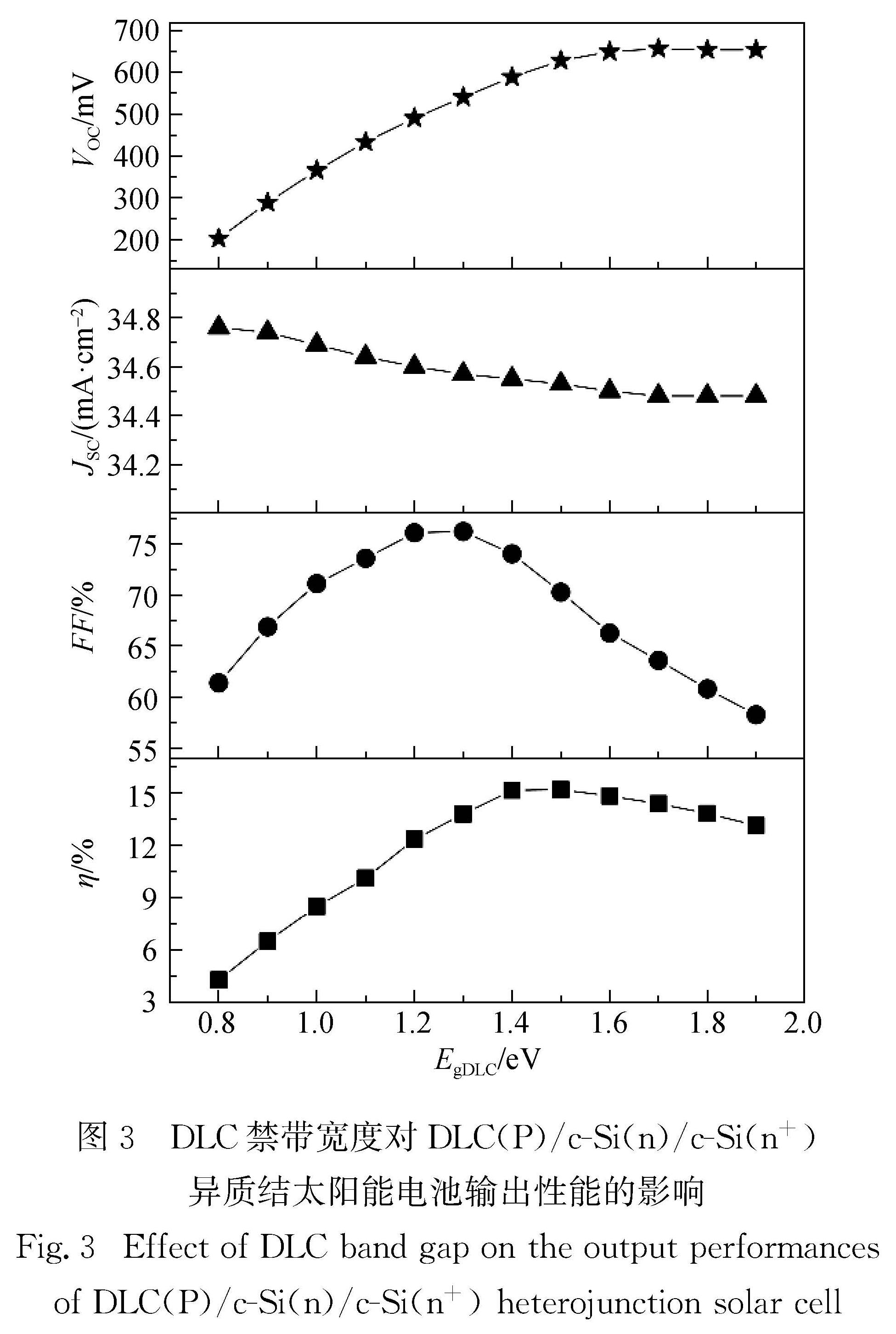
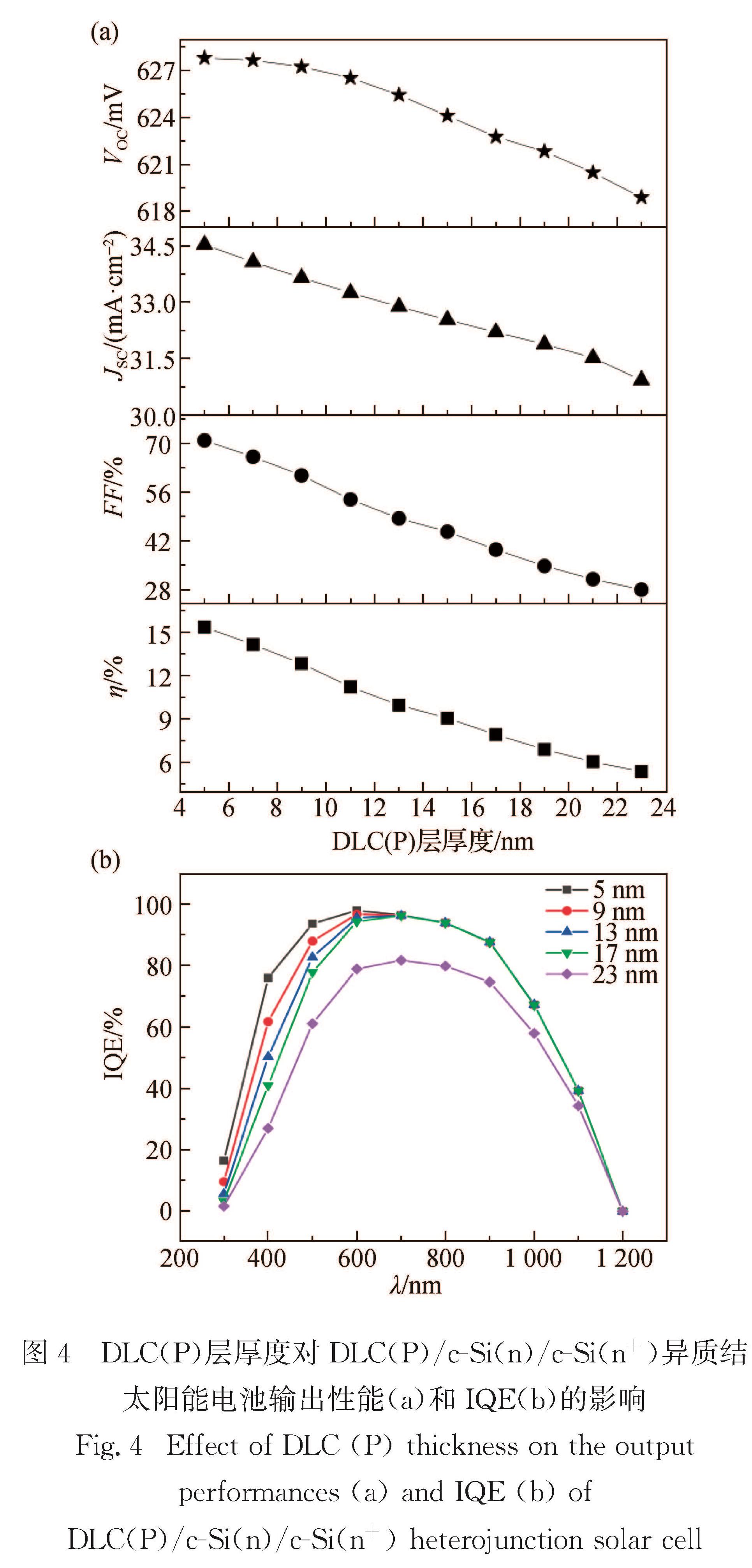
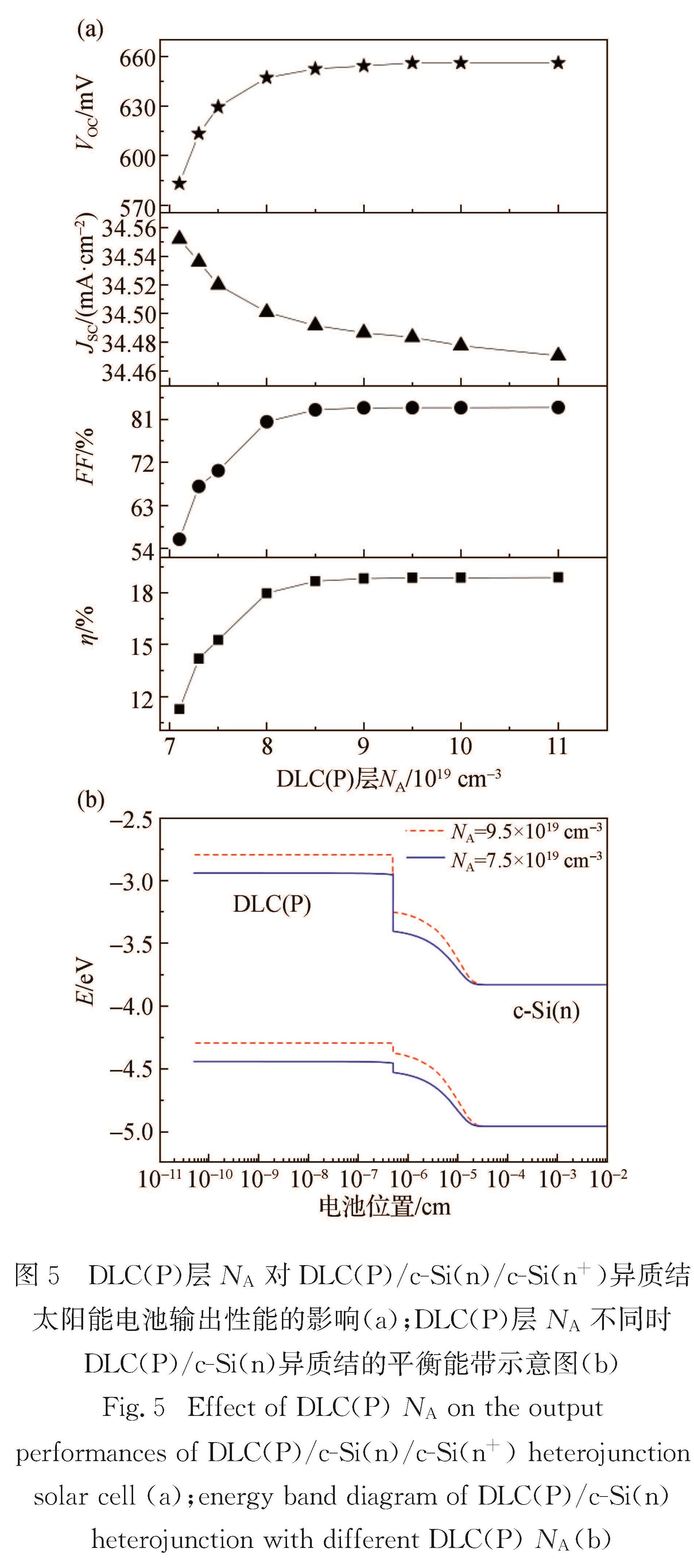
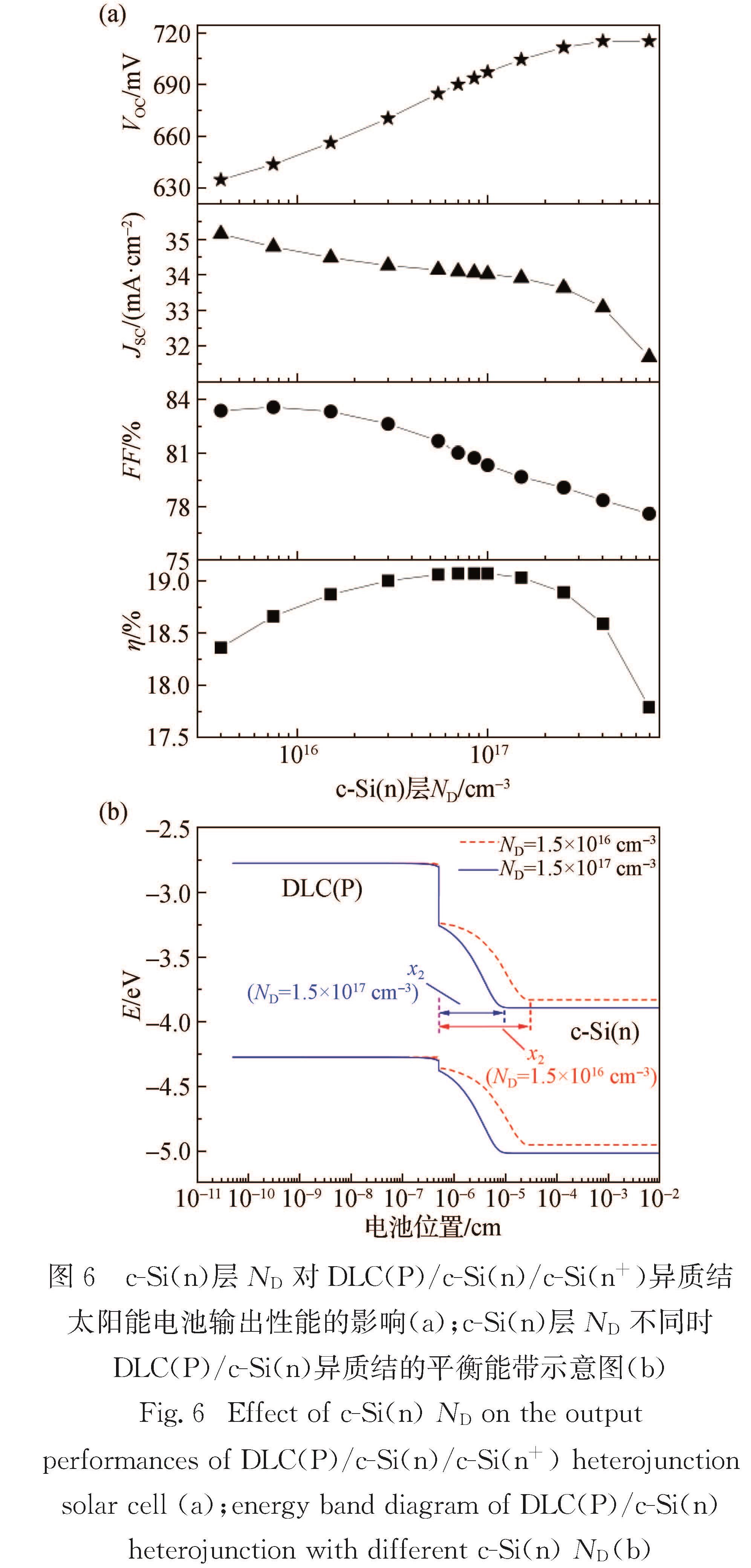
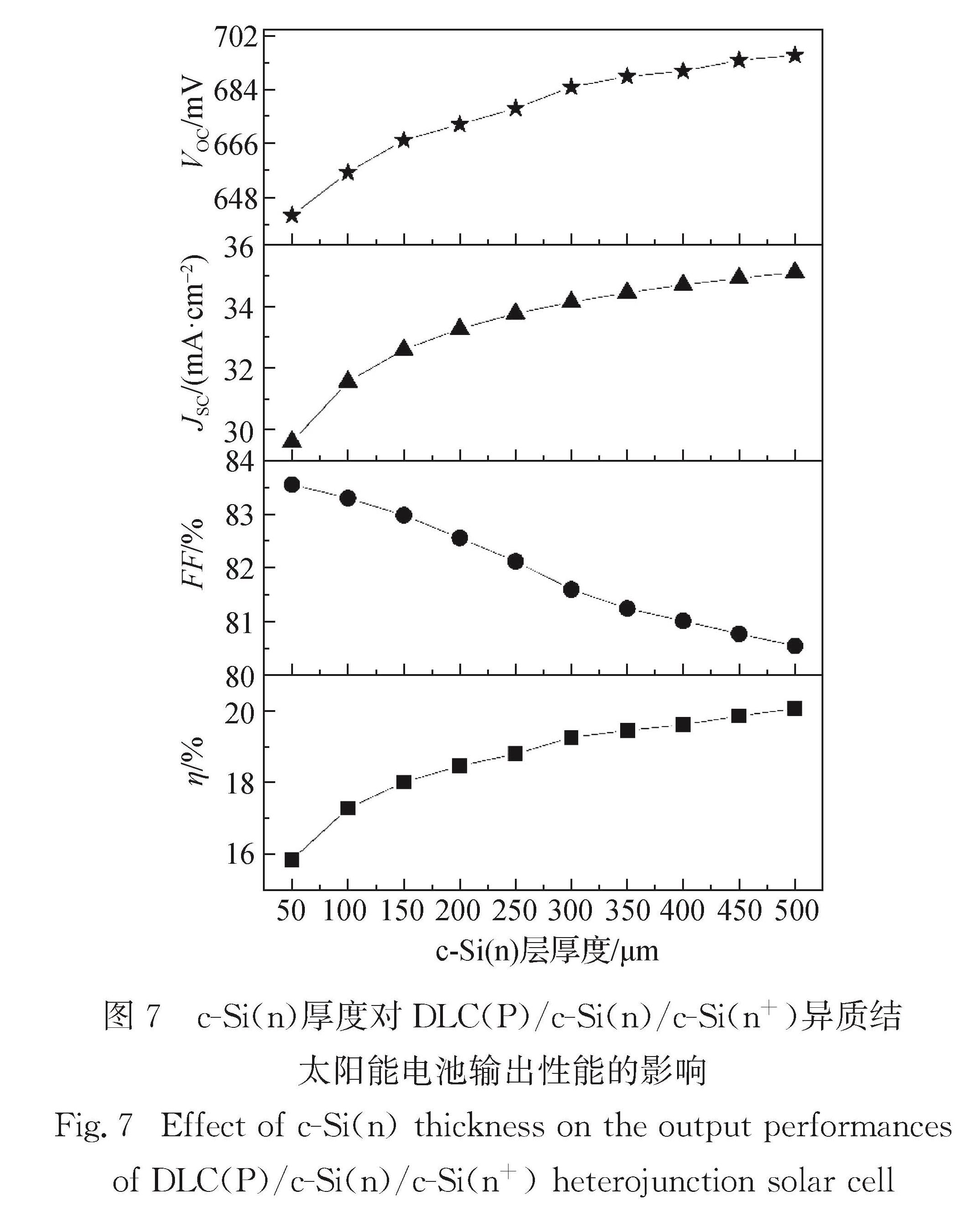
Results :The results show that the photoelectric conversion efficiency of the solar cell with this structure increased first and then decreasedwith an increasein the band gap width of the DLC(P) layer. When the band gap width of the DLC(P) layer was 1.5eV, the conversion efficiency reached the maximum. To find out the correlation between the thickness of the DLC(P) layer and the conversion efficiency, a simulation experiment wasconducted to change the thickness of the DLC(P) layer with a fixed band gap width of 1.5eV.It was found that the conversion efficiency decreasedwiththe thickness of the DLC(P) layer. Since the thickness of the DLC(P) layer cannot be infinitely thin during the actual preparation process and the thinnest DLC had been preparedto be5nm thick, we took a band gap width of the DLC(P) layer of 1.5eV and a thickness of 5nm to study the effect of the doping concentration on the conversion efficiency. The results show that an increase in the doping concentration moved the Fermi level to the top of the valence band, the quasi Fermi energy level difference of heterojunction augmented, andthe open circuit voltagerose, leading to animprovement of the conversion efficiency. Similarly, we studied the effect of the doping concentration of the c-Si(n) layer on the conversion efficiency of DLC/c-Si(n)/c-Si(n+) heterojunctionsolar cells.We found that when the level ofthe doping concentration of the c-Si(n) layer was 5.5×1016cm-3, we got a maximum conversion efficiency of the DLC/c-Si(n)/c-Si(n+) heterojunction solar cell. The increase in the thickness of the c-Si(n) layer improved the photoelectric conversion efficiency, while the cost of preparation of the DLC(P) layer variedwith different thickness.The thickness of the c-Si(n) layer could be controlled according to actual needs.
Conclusion s:When the band gap width of the DLC(P) layer was 1.5eV, the thickness of the DLC(P) layerwas 5 nm, the acceptor doping concentration was 9.5×1019cm-3, the thickness of c-Si(n) layer was 500 μm and the donor doping concentration was 5.5×1016cm-3, the conversion efficiency of the DLC(P)/c-Si(n)/c-Si(n+) heterojunction solar cell could reach 20.07% (open circuit voltage was 695.5 mV, short circuit current density was 35.11 mA/cm2, the fill factor was 80.56%).It is worth mentioning that the interface state defect density of the DLC(P) / c-Si(n) layer deserves close attention, since the interface defect may produce energy levels in the band gap, which leads to serious carrier recombination and greatly reduces the conversion efficiency of the DLC/c-Si heterojunction solar cell. Therefore, in the actual preparation process, efforts should be made to reduce the interface state defect density of the DLC(P)/c-Si(n) layer in order to obtain a greater conversion efficiency.Due to complex and changeable structure of DLC, stable preparation of DLC and reduction of the interface state defect density of the DLC(P)/c-Si(n) layer still face technical problems. However, from the above simulation results, it can be seen that if these technical bottlenecks can be broken through, DLC/Si heterojunction solar cellswill have a broader application in high radiation environments such as the space.